大綱 CPLD 簡介與市場現狀 EDA 工具 -MAX+plusII 圖形設計快速入門 -Graphic 圖形編輯的階層式設計 霹靂燈實習 文書設計快速入門 -VHDL Graphic 與 VHDL 整合
|
|
|
- 览晃 嵇
- 6 years ago
- Views:
Transcription
1 CPLD/VHD 淡江大學電機系微處理機實
2 大綱 CPLD 簡介與市場現狀 EDA 工具 -MAX+plusII 圖形設計快速入門 -Graphic 圖形編輯的階層式設計 霹靂燈實習 文書設計快速入門 -VHDL Graphic 與 VHDL 整合
3 CPLD 簡介與市場現
4 PLD 簡介
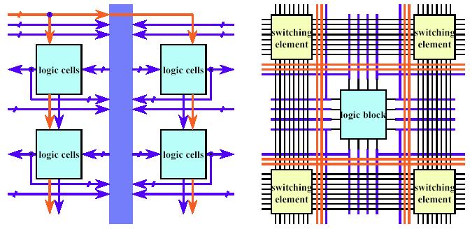
5 可程式化元件的內部連線 CPLD FPGA
6 CPLD 架構 以 Altera MAX7000 系列之基於乘積項 (Product-Term) 的 PLD 內部架構 這種 PLD 可分為三塊架構..宏單元 (Macrocell), 可編程連線 (PIA) 和
7 可編 Marocell 架構 乘積項陣列 可編程選擇開關
8 基於乘積項結構的 CPLD 邏輯實現範 f ( A B) C D ( A C D) ( B C D)

9 每個 LAB 由 FPGA 架構 -Altera FLEX10K 內部結構
10 EAB 內部構造
11 LAB 內部構造
12 邏輯單元 (LE) 內部結構
13 基於 LUT 結構的 FPGA 邏輯實現範例 A,B,C,D 由 FPGA 晶片的 IOE 進入 PIA, 然後作為 LUT 的位址線位址查找到相對應的數值作為輸出 直接利用 LUT 後面 D 型正反器來實現 D 型正反器 CLK 由 I/O 腳輸入後進入晶片內部的 clock 專用通道, 直接連接器的 clock 端 正反器的輸出與 I/O 腳相連, 把結果輸出到晶片 IOE


14 FPGA/CPLD 設計流程 Design Ideas Detailed Design Functional Simulation Device Programming Timing Simulation Implementation (P&R) FPGA CPLD t pd =22.1ns f max =47.1MHz

15 可程式化元件 我們可隨時利用 download cable 或 hardware programmer 下載實驗板上的 FPGA/CPLD 來驗證我們的設計


16 FPGA/CPLD 應用 Digital Video Techologies FPGA/CPLD Test / Measurement Robot
17 FPGA/CPLD 市場現況 This Course 供應商產品最新開 Altera Xilinx Lattice Actel MAX, FLEX, APEX, Stratix, Cyclone, MAXII website: XC9500, CoolRunner, Spartan, Virtex website: ispxpld, ispmach, ispxpga, ORCA website: ex, SX, MX, Axcelerator, ProASIC website: MAX+plu QuartusII ISE 7.1i isplever Libero IDE
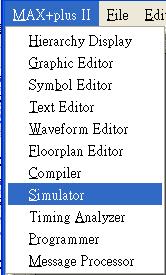
18 EDA 工具 -MAX+plu

19 MAX+plus II MAX+PLUS II Text Editor MAX+PLUS II Waveform Editor MAX+PLUS II Floorplan Editor Design Entry MAX+PLUS II Graphic Editor MAX+PLUS II Symbol Editor Project Verification CNF Extractor SNF Extractor Netlist Writer MAX+PLUS II Message Processor & Hierarchy Display Project Processing MAX+PLUS II Compiler Database Builder Partitioner Design Doctor Logic Synthesize Fitter Assembler Device Programming MAX+PLUS II Simulator MAX+PLUS II Timing Analyzer MAX+PLUS II Waveform Editor MAX+PLUS II Programmer

20 MAX+plus II --- Design Entry

21 MAX+plus II --- Project Processing

22 MAX+plus II --- Project Verification

23 MAX+plus II --- Device Programmin
24 實驗平台 --- FPT-3 採用 Altera CPLD 的 MAX7000S 系列元件 EPM7064SLC44-10 EEPROM 架構的 PLD 5V 工作電壓 可支援 1250 個邏輯閘,64 個 LCs 可使用 32 個 I/O 系統電源 :5 伏特直流 輸出介面 系統時脈 :1.8432MHz LED( 低電位驅動 ) ISP 燒錄介面輸入介面 邏輯準位指撥開關 2 位數七段顯示器 ( 共陽極動 ) 1 組高效能蜂鳴器 4 組負脈衝無段式按鍵開關

25 實驗平台 --- LP-2900
26 實驗平台 --- LP-2900 採用 Altera FLEX10K 系列元件 EPF10K10TC144-4 支援大約 閘的設計 下載資料至 FPGA 元件的方式 ByteBlaster 下載 ( 使用 PC 的 LPT Port) EPROM 下載 ( 須先將資料燒錄至 EPROM) 使用 PrintPort 下載 準備 *.sof 檔案 ( 編譯後會自動產生 ) 執行 :MAX+Plus2->Programmer->File->Select Program F 範例 : C:\Leap-2900\*.sof 使用 EPROM 下載 將 *.hex 檔案燒綠至 EPROM 中 將 EPROM 置入 AU3 IC 座 按 RESET 鍵一次
27 圖形設計快速入門 Graphic

28 圖形設計快速入門 1/7 File New, 選擇圖形編輯檔 (Gra Editor file)

29 圖形設計快速入門 2/7 File Save as, 將編輯檔案命名 halfadd.gdf 存入指定的資料夾中 ( 不可將檔放於根目錄下, 且資料夾名稱不可以為中文
30 圖形設計快速入門 3/7 File Project Set Project to Cu File, 將專案 (project) 名稱設定成與現在所的檔案名稱一致

31 在視窗中用滑鼠左鍵快速連或 Symbol Enter S 出現 Enter Symbol 的對話窗 圖形設計快速入門 4/7 選擇..\maxplus2\max2lib\prim 元件庫內的邏

32 圖形設計快速入門 5/7 輸入 xor and2 input 及 output 等 symbol
,")
33 細線代表一般線, 粗線則是 圖形設計快速入門 6/7 元件腳位的連線 繪圖工具列可供使用者選擇使用 腳位的線條連接可在起點按住 ( 此時會出現十字形游標 ), 拖曳到適當的位置放開即可完

34 圖形設計快速入門 7/7 輸入與輸出腳位的命名 以滑鼠左鍵點選 PIN_NAME 的地方, 當文字部黑色編輯方塊時即可重新輸入字元或更改檔名中每一個輸入輸出腳位都應有一個獨立的名稱


35 檔案的編繹 1/2 儲存 檢查和簡易編繹 File Project Save & Check


36 檔案的編繹 2/2 進行簡易的編繹 Processing Functional SNF Extractor 在 Compiler 視窗下按 Start

37 功能編譯處理程序 Compiler Netlist Extractor 產生.cnf 檔, 檢查程式是否正確 Database Builder 建構節點名稱資料庫 Functional SNF Extractor 產生提供功能模擬使用之.snf 檔

38 電路的功能模擬 1/6 開啟一個新的檔案 File New Waveform Editor file 儲存檔名, 選擇 File 將該 Waveform 檔存於所建立夾裡, 檔名與專案名稱相同 ( *.scf)


39 電路的功能模擬 2/6 設定模擬時間 File End Time 設定格線間距 Options Grid Size 顯示格線 Options Show Grid

40 電路的功能模擬 3/6 輸入所欲分析的電路節點 Node Enter Nodes from SNF

41 電路的功能模擬 4/6 放大波形縮小波形將整體波形放入畫面中將選取區設定為 Low 訊號將選取區設定為 High 訊號將選取區設定為 Unknown 訊號將選取區設定為高組抗訊號將選取區波形反向自動時脈產生鈕自動計數產生鈕設定選取區之群組值設定選取區之狀態值

42 電路的功能模擬 5/6 輸入腳位的波形定義 使用視窗左側工具列來協助完成我們想要的數位形式 ; 首先將要設定的區域選取, 這時候會形成一段標示反白的區域, 再選擇工具列裡所要的數位脈衝 (High 或 Lo 即可完成輸入訊號波形的設定

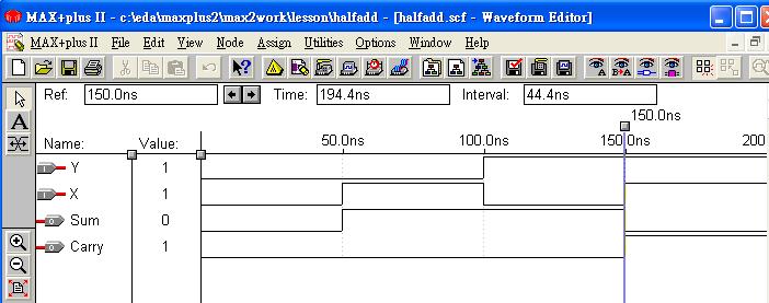
43 電路的功能模擬 6/6 執行模擬 Max+plusII Simulator, 按下 Start

44 時序分析器 (Timing Analyzer) 的使 重新編繹 File Project Save & Check 在 Processing 下取消 Functional SNF Extractor 的勾選完整的編繹, 此時時序的模擬結果便會加入延遲的因素考量


45 時序分析器 (Timing Analyzer) 的使 MAX+plusII Timing Analyer 按下 Delay Matrix 下的 Start 鈕即可得到所有節點之間的延遲分析結果

46 時序編譯處理程序 Compiler Netlist Extractor and Database Builder 檢查程式語法與建立電路描述檔資料庫 Logic Synthesizer 電路合成與電路最佳化 Partitioner and Fitter 執行電路佈局與繞線演算法, 產生.rpt 檔 Timing SNF Extractor 產生提供時序模擬使用之.snf 檔 Assembler 產生供元件下載用之檔案

47 建立電路符號檔 File Create Default Symbol File Edit Symbol


48 平面配置與晶片規劃 1/4 選取晶片型號 Assign Device MAX7000S EPM7064SLC44-10 取消 Show Only Fastest Speed Grades 選項以顯示更多

49 平面配置與晶片規劃 2/4 再作一次完整的編繹程序 點選 rpt 文件圖示以開啟 halfadd.rpt 檔案


50 平面配置與晶片規劃 3/4 MAX+plusII Floorplan Editor Layout Device View Layout Current Assignments Floorplan ( 或是透過視窗左邊的工具列點選 )

51 平面配置與晶片規劃 4/ X Y 設計積體電路外觀示意圖與晶片腳位配置 完成腳位配置後必須再作一次完整的編繹程序 EPM7064SLC 以滑鼠拖曳的方式將各接腳依規劃需求拖到晶片的 I/O 腳位


52 程式下載與測試 1/3 開啟 programmer 視窗 MAX+plus II Programmer Programming hardware is not installed 警示視窗


53 程式下載與測試 2/3 Options Hardware Setup, 選取 Hardw Type 至 ByteBlaster(MV), 點選 OK
 File Select Programming File 按下 Program")
54 程式下載與測試 3/3 選擇所欲燒錄的.pof 檔 (halfadd.pof) File Select Programming File 按下 Program 以執行程式下載動作
55 圖形設計快速入門 --- FPT-3 驗證 SUM Carry XY
56 圖形編輯的階層式設
57 Carry 圖形編輯的階層式設計 1/4 以半加器和 OR 閘建構全加器 Full Adder U1 Half Adder U2 Half Adder X Y Sum U3 Z


58 圖形編輯的階層式設計 2/4 開啟新的圖形編輯檔案, 加入兩個 halfadd 這前所建立的 Symbol 與一個 or2 邏輯閘


59 圖形編輯的階層式設計 3/4 完成元件間的連線關係, 並修改腳位名稱 將檔案存成 fulladd.gdf, 並將專案名稱設定成與檔名一致, 進行程式編繹與功能模擬
 SUM Y 31(dip2) Carry Z 33(dip3)")
60 圖形編輯的階層式設計 4/4 選取晶片型號 MAX7000S EPM7064SLC44-10 腳位配置 輸入腳位輸出 X 29(dip1) SUM Y 31(dip2) Carry Z 33(dip3) 程式下載與測試
61 圖形編輯的階層式設計 --- FPT-3 驗證 SUM Carry XYZ
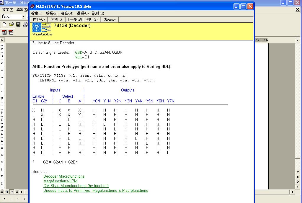
62 直接套用 MAX+plus II 中的 74 系列元 介紹如何直接使用 MAX+plus II 所提供的 Macro Fun 元件庫來繪製電路圖 從 Help Old-Style Macrofunctions 線上資的資料中, 我們可以查看元件的詳細規格

63 74138 解碼器元件的使用
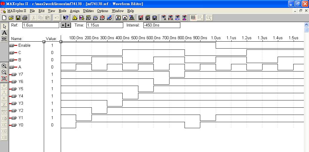
64 繪製電路圖與功能模擬
65 霹靂燈實習
 4count(4 位元上 / 下數計數器 ) 74138( 碼器 ) vcc gnd")
66 霹靂燈實習 1/3 完成一個具有重置 右旋 左旋等功能之霹靂燈實習 1. 輸入 74292( 除頻器 ) 4count(4 位元上 / 下數計數器 ) 74138( 碼器 ) vcc gnd not input 及 output 等 symbol
67 霹靂燈實習 2/3 2. 完成連線與腳位的命名 3. 儲存檔案 (led.gdf)
68 霹靂燈實習 3/3 4. 選取晶片型號 MAX7000S EPM7064SLC 腳位配置 輸入腳位輸出 CLK 43(clk) L1 RST 37(PS1) L2 6. 程式編譯 下載與測試 DnUp 29(SW1) L3 L4 L5 L6 L7 L8
69 文書設計快速入門 VHDL
70 VHDL 快速入門
71 A simple example 8-bit compar --An Example VHDL Code library IEEE; use IEEE.std_logic_1164.all; entity cmp8 is port( A: in std_logic_vector(7 downto 0); B: in std_logic_vector(7 downto 0); EQ: out std_logic); end Cmp8; architecture dataflow of cmp8 is begin eq <= 1 when (a = b) else 0 ; end dataflow; 不分大小寫 註解 : '--' 敘述結尾 : 等號 : '<=' 使用者定義名 字母 數字 需由字母開 不分大小寫 不能使用 V 最後字元不 兩個 _ 不
72 VHDL 五大元素 Entity Block 的 I/O 規格 Architecture block 的內部電路 可同時存在多個 Configuration 決定那一個 architecture 被使用 Package Package body Arch1 (version 1) Entity Arch2 (version 2
73 第一元素 Entity Entity Name Entity NAND2 is port (A, B : in std_logic; Z : out std_logic); Data Type end nand2; I/O Direction A B NAND2 Z
74 I/O Direction IN OUT INOUT BUFFER
75 Basic Data Type Bit BIT_VECTOR (0 TO 7) STD_LOGIC STD_LOGIC_VECTOR (15 DOWNTO 0)
76 第二元素 NAND2 architecture Architecture Structure of NAND2 is signal C : std_logic; begin U0 : and2x1 port map (A, B, C); U1 : invx1 port map (C, Z); end Structure; A B And (and2x1) NAND2 C Invert (invx U0 U1
77 第二元素 NAND2 architecture Architecture DataFlow of NAND2 is begin Z <= A nand B; -- concurrent statement end DataFlow;
78 第二元素 AND2 architecture # Architecture RTL of NAND2 is begin process(a, B) begin if (A= 1 ) and (B= 1 ) then --sequential statem Z<= 0 ; else Z<= 1 ; end if; end process; end RTL;
79 第三元素 Configuration Configuration cfg_nand2 of NAND2 is for RTL end for; end cfg_nand2; A B RTL Z
80 Recall Entity a IS XXX END a; ARCHITECTURE b Of a IS BEGIN XXX END b; CONFIGURATION c OF a IS FOR b END FOR; END c;
81 第四 五元素 Package Package Declarations Package Bodies Constant Declarations Subprograms Type Declarations Component Declarations
82 Package Package EXAMPLE is type BYTE is range 0 to 255; subtype NIBBLE is BYTE range 0 to 15; constant BYTE_FF: BYTE:=255; signal ADDEND: NIBBLE; component BYTE_ADDER port(a,b: in BYTE; C: out BYTE; OVERFLOW: out BOOLEAN); end component; function MY_FUNCTION(A: in BYTE) return BYTE; end [EXAMPLE];
83 Using Package library IEEE; use IEEE.std_logic_1164.ALL; use IEEE.numeric_std.ALL; use IEEE.std_logic_arith.ALL; use IEEE.std_logic_unsigned.ALL; use IEEE.std_logic_signed.ALL; - - Library WORK; use WORK.EXAMPLE.ALL; entity... architecture...

84 文書設計快速入門 --- 霹靂燈實習 top_vhd.vhd clk_div.vhd counter.vhd decoder.vhd CLK 除頻器 計數器 3 對 8 解碼器 10Mhz 10hz 3 8 RST DnUp


85 文書設計快速入門 1/4 File New, 選擇文書編輯檔 (Text Editor file) File Save as, 將編輯檔案命名為 clk_div.vhd 存入資料夾中


86 文書設計快速入門 2/4 完成除頻器之 VHDL 程式 可改變除頻的倍數


87 文書設計快速入門 3/4 File Project Set Project to Current File, 將專 (project) 名稱設定成與現在所編輯的檔案名稱一致 File Project Save and Check, 儲存檔案並檢語法


88 文書設計快速入門 4/4 確定程式語法無誤 進行簡易的編繹

89 電路的功能模擬 1/7 開啟一個新的 Waveform Editor, 並將 clk_in clk_o cnt1 信號加入, 並儲存為 clk_div.scf 檔

90 電路的功能模擬 2/7 Option Grid Size, 將單位時間長度設定


91 電路的功能模擬 3/7 File End Time, 將模擬時間設定為 10


92 電路的功能模擬 4/7 點選 clk_in 使其反白, 並按下 Clock 圖示以產生
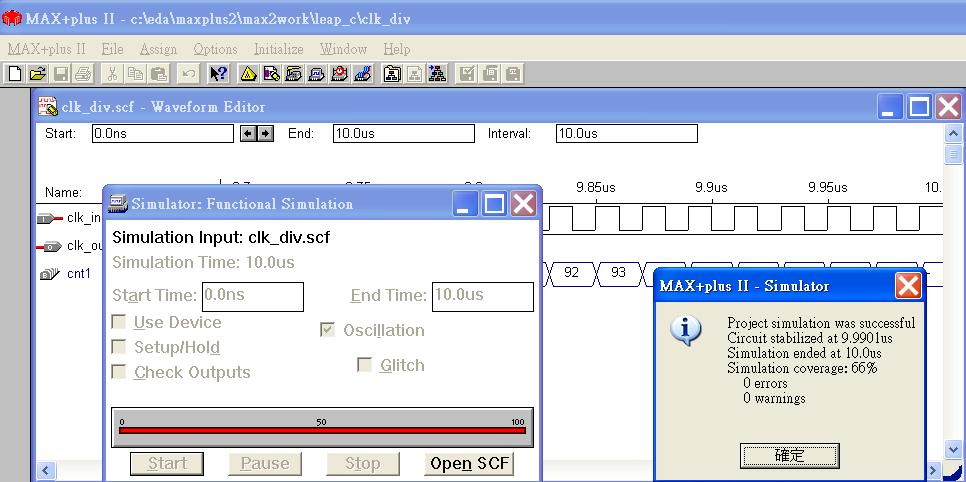
93 電路的功能模擬 5/7 點選功能模擬圖示以完成模擬動作
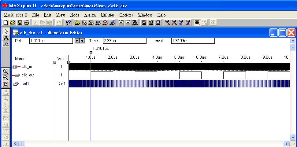
94 電路的功能模擬 6/7 點選圖示將畫面顯示成整體時間長度


95 電路的功能模擬 7/7 將畫面放大, 可驗證出 clk_out 的頻率為 clk_in 除以 1
96 計數器程式碼 實驗名稱 : 霹靂燈實習 -- 檔案名稱 :counter.vhd -- 功能 :3 位元上 / 下數計數器 -- 日期 : library ieee; use ieee.std_logic_1164.all; use ieee.std_logic_unsigned.all; entity counter is port( CLK : in std_logic; RST : in std_logic; DnUp : in std_logic; CNT : out std_logic_vector(2 downto 0) ); end counter; process (CLK,RST,DnUp) begin if RST = '0' then cnt1 <= "000"; elsif CLK'event and CLK='1' then if DnUp='1' then cnt1 <= cnt1-1; else cnt1 <= cnt1 + 1; end if; end if; end process; CNT <= cnt1; end a; architecture a of counter is signal cnt1 : std_logic_vector(2 downto 0); begin
97 3 對 8 解碼器程式碼 實驗名稱 : 霹靂燈實習 -- 檔案名稱 :decoder.vhd -- 功能 :3 對 8 解碼器 -- 日期 : library ieee; use ieee.std_logic_1164.all; use ieee.std_logic_unsigned.all; entity decoder is port( A : in std_logic; B : in std_logic; C : in std_logic; Y : out std_logic_vector(7 downto 0) ); end decoder; architecture a of decoder is signal XIN : std_logic_vector(2 downt begin XIN <= C & B & A; with XIN select Y <= " " when "000", " " when "001", " " when "010", " " when "011", " " when "100", " " when "101", " " when "110", " " when "111", " " when others; end a;
98 主程式程式碼 實驗名稱 : 霹靂燈實習 -- 檔案名稱 :top_vhdl.vhd -- 功能 : 霹靂燈主程式 -- 日期 : library ieee; use ieee.std_logic_1164.all; use ieee.std_logic_unsigned.all; entity top_vhdl is port( CLK : in std_logic; RST : in std_logic; DnUp : in std_logic; L : out std_logic_vector(8 downto 1); LED_COM : out std_logic ); end top_vhdl; architecture a of top_vhdl is component clk_div generic(divisor:integer:= ); port( clk_in : in std_logic; clk_out: buffer std_logic ); end component; 將專案名稱設定為主程式名稱 --- component counter port( CLK : in std_logic; RST : in std_logic; DnUp : in std_logic; CNT : out std_logic_vector(2 downto 0) ); end component; component decoder port( A : in std_logic; B : in std_logic; C : in std_logic; Y : out std_logic_vector(7 downto 0) ); end component; signal clk_10hz : std_logic; signal CNT_t : std_logic_vector(2 downto 0); begin LED_COM <= '1'; U1 : clk_div port map(clk,clk_10hz); U2 : counter port map(clk_10hz,rst,dnup,cnt_ U3 : decoder port map(cnt_t(0),cnt_t(1),cnt_t end a;
 L1 RST 37(PS1) L2 程式編譯 下載與測試 DnUp 29(SW1) L3 L4 L5 L6")
99 檔案的編繹與驗證 選取晶片型號 MAX7000S EPM7064SLC44-10 腳位配置 輸入腳位輸出 CLK 43(clk) L1 RST 37(PS1) L2 程式編譯 下載與測試 DnUp 29(SW1) L3 L4 L5 L6 L7 L8

100 Graphic 與 VHDL 整合 開啟新的圖形設計檔 (Graphic Editor), 可將 VHDL 編譯後的 S 入並加以連線, 以完成整合 Graphic 與 VHDL 之系統設計
101 Graphic 與 VHDL 整合 完成以下之電路連線後並儲存檔案為 top_graphic.g 將專案名稱設定為 top_graphic 並完成系統編譯與驗
102 參考資料 陳慶逸 林柏辰編著,VHDL 數位電路實習與專題設文魁資訊,2005
103 Click below to find more Mipaper at Mipaper at
a b c d e f g C2 C1 2
 a b c d e f g C2 C1 2 IN1 IN2 0 2 to 1 Mux 1 IN1 IN2 0 2 to 1 Mux 1 Sel= 0 M0 High C2 C1 Sel= 1 M0 Low C2 C1 1 to 2 decoder M1 Low 1 to 2 decoder M1 High 3 BCD 1Hz clk 64Hz BCD 4 4 0 1 2 to 1 Mux sel 4
圖形編輯設計簡介 建立電路符號檔與轉換成VHDL程式碼 2
 圖形編輯設計法 圖形編輯設計簡介 建立電路符號檔與轉換成VHDL程式碼 2 建立電路符號檔 1.執行 File Create/ Update Create Symbol Files for Current File 時 可將目前的半加法器建立一個電路符號 Halfadd.bsf 3 建立電路符號檔 2.利用 File Open 開啟Halfadd.bsf檔案時 便可查看所建 立的電路符號 Halfadd
B 6 A A N A S A +V B B B +V 2
 B 6 A A N A S A +V B B B +V 2 V A A B B 3 C Vcc FT7 B B 1 C 1 V cc C 2 B 2 G G B 3 C 3V cc C B ND ND GND V A A B B C 1 C 3 C 2 C V cc V cc V 220Ωx B 1 B 2 B 3 B GND GND A B A B 1 1 0 0 0 2 0 1 0 0 3 0
前言
 FPGA/CPLD FPGA/CPLD FPGA/CPLD FPGA/CPLD FPGA/CPLD 1.1 FPGA/CPLD CPLD Complex Programable Logic Device FPGA Field Programable Gate Array 1.3 CPLD/FPGA PLD PLD ASIC PLD PLD PLD FPGA PLD 7032LC 3 PLD 70 1
(Microsoft Word - \245\274\244\300\246\250\301Z\260\252\247C13.doc)
") VHDL 實 習 報 告 四 資 工 二 指 導 教 授 : 徐 演 政 學 生 : 廖 雅 竹 B9515010 陳 緯 琪 B9515044 敗 LED 史 上 無 敵 超 級 賭 骰 子 模 擬 機 以 廖 雅 竹 陳 緯 琪 Project Title: 骰 硬 件 啟 動 後, 可 以 明 顯 的 觀 察 到 實 驗 板 上 方 的 兩 個 骰 子 器 高 速 地 跳 動 Participants:
VHDL 實 習 報 告 四 資 工 二 指 導 教 授 : 徐 演 政 學 生 : 廖 雅 竹 B9515010 陳 緯 琪 B9515044 敗 LED 史 上 無 敵 超 級 賭 骰 子 模 擬 機 以 廖 雅 竹 陳 緯 琪 Project Title: 骰 硬 件 啟 動 後, 可 以 明 顯 的 觀 察 到 實 驗 板 上 方 的 兩 個 骰 子 器 高 速 地 跳 動 Participants:
 USB - 1 - - 2 - - 3 - - 4 - - 5 - - 6 - - 7 - DES Module FSM CONTROLLER 8 6 8 Key ROM 8 8 Data_in RAM Data_out RAM 8 USB Board - 8 - - 9 - - 10 - - 11 - - 12 - USB device INF Windows INF Device Function
D-Type entity D_FF is D :in std_logic; CLK :in std_logic; Q :out std_logic); end D_FF; architecture a of D_FF is process(clk,d) if CLK'EVENT and CLK =
; end D_FF; architecture a of D_FF is process(clk,d) if CLK'EVENT and CLK =") VHDL (Sequential Logic) D-Type entity D_FF is D :in std_logic; CLK :in std_logic; Q :out std_logic); end D_FF; architecture a of D_FF is process(clk,d) if CLK'EVENT and CLK = '1' then Q
VHDL (Sequential Logic) D-Type entity D_FF is D :in std_logic; CLK :in std_logic; Q :out std_logic); end D_FF; architecture a of D_FF is process(clk,d) if CLK'EVENT and CLK = '1' then Q
(Load Project) (Save Project) (OffLine Mode) (Help) Intel Hex Motor
 (Save Project) (OffLine Mode) (Help) Intel Hex Motor") 1 4.1.1.1 (Load) 14 1.1 1 4.1.1.2 (Save) 14 1.1.1 1 4.1.2 (Buffer) 16 1.1.2 1 4.1.3 (Device) 16 1.1.3 1 4.1.3.1 (Select Device) 16 2 4.1.3.2 (Device Info) 16 2.1 2 4.1.3.3 (Adapter) 17 2.1.1 CD-ROM 2 4.1.4
1 4.1.1.1 (Load) 14 1.1 1 4.1.1.2 (Save) 14 1.1.1 1 4.1.2 (Buffer) 16 1.1.2 1 4.1.3 (Device) 16 1.1.3 1 4.1.3.1 (Select Device) 16 2 4.1.3.2 (Device Info) 16 2.1 2 4.1.3.3 (Adapter) 17 2.1.1 CD-ROM 2 4.1.4
untitled
 2004-2-16 (3-21) To Luo 207 Xilinx FPGA/CPLD ISE Xilinx Integrated Software Environment 6.1i FPGA VHDL VerilogHDL EDIF ModelSim FPGA FPGA ISE HDL FPGA ISE 7.1 7.1.1 ISE6.1i ISE6.1i ISE ModelSim ISE ModelSim
B3B2B1B0 CA CB CC CD CE CF CG
 Lab7:7 段顯示器控制電路 [ 實驗說明 ] : 這一個範例將分成兩階段 首先使用 ISE12.4 先進行叫用 Seven_Segmenet.vhd 模組建立 4bit HEX 轉換 7 段顯示器控制電路練習 接著再使用 Lab1 所設計的 2:4 解碼器與 Lab4 四位元加法器電路利用 Schematic 階層式設計快速建立加法器和輸出到 7 段顯示器的控制電路 你將開啟一個 Seven_Segmenet_Adder.sch
目录
 ALTERA_CPLD... 3 11SY_03091... 3 12SY_03091...4....5 21 5 22...8 23..10 24..12 25..13..17 3 1EPM7128SLC.......17 3 2EPM7032SLC.......18 33HT46R47......19..20 41..20 42. 43..26..27 5151DEMO I/O...27 52A/D89C51...28
图 片 展 示 : 资 源 简 介 : FPGA Altera CycloneII EP2C5T144C8 (4608 个 LE) 2 路 有 源 晶 振 (50M,25M) AS & JTAG 标 准 接 口 VGA 接 口 UART 接 口 蜂 鸣 器 8bit 并 行 DAC 8 路 按 键
 2 路 有 源 晶 振 (50M,25M) AS & JTAG 标 准 接 口 VGA 接 口 UART 接 口 蜂 鸣 器 8bit 并 行 DAC 8 路 按 键") 官 方 淘 宝 地 址 :http://metech.taobao.com/ MeTech verilog 典 型 例 程 讲 解 V1.0 笔 者 :MeTech 小 芯 技 术 支 持 QQ : 417765928 1026690567 技 术 支 持 QQ 群 :207186911 China AET 讨 论 组 http://group.chinaaet.com/293 笔 者 博 客 :http://blog.csdn.net/ywhfdl
官 方 淘 宝 地 址 :http://metech.taobao.com/ MeTech verilog 典 型 例 程 讲 解 V1.0 笔 者 :MeTech 小 芯 技 术 支 持 QQ : 417765928 1026690567 技 术 支 持 QQ 群 :207186911 China AET 讨 论 组 http://group.chinaaet.com/293 笔 者 博 客 :http://blog.csdn.net/ywhfdl
目 录
 1 Quick51...1 1.1 SmartSOPC Quick51...1 1.2 Quick51...1 1.3 Quick51...2 2 Keil C51 Quick51...4 2.1 Keil C51...4 2.2 Keil C51...4 2.3 1 Keil C51...4 2.4 Flash Magic...9 2.5 ISP...9 2.6...10 2.7 Keil C51...12

 ... 3... 9... 9... 32... 49... 69... 94... 125... 157... 186... 199... 210... 251... 269... 279... 293... 311... 325... 344... 361... 379... 398... 415... 441... 441... 443 ... 445... 447... 449... 451...


2
 1 2 3 5 20 45 87 137 137 138 139 140 141 1 2 3 4 5 6 7 8 9 10 11 12 13 14 15 16 17 18 19 20 21 22 23 24 25 26 27 28 29 30 31 32 33 34 35 36 37 38 39 40 41 42 43 44 45 46 47 48 49 50 51 52 53 54 55 56 57

!"# $! "##$! $ "%& % & #$# & ()% & "!! * "! * #! * * $! ((!"# "##$ + #++ * * * * * * * * * * + $," ("# +### "##$ $ + + & $ ### "%& % & #$# & ()% & " "
% & !! * ! * #! * * $! ((!# ##$ + #++ * * * * * * * * * * + $, (# +### ##$ $ + + & $ ### %& % & #$# & ()% &") "!!!!!!!!!!!!!!!!!!!!!!!!!!!!!!!!!!!!!!!!!!!!!!!!!!!!!!! "!!!!!!!!!!!!!!!!!!!!!!!!!!!!!!!!!!!!!!!!!!!!!!!!!!!!!!!!!!!!!!!!!!!!!!!!!!!!!!!!!!!!!!!!!!!!!!!!!!!!!!!!!!!!!!!!!!!!!!!!!!!!!!!!!!!!!!!!!!!!!!!!!!
"!!!!!!!!!!!!!!!!!!!!!!!!!!!!!!!!!!!!!!!!!!!!!!!!!!!!!!! "!!!!!!!!!!!!!!!!!!!!!!!!!!!!!!!!!!!!!!!!!!!!!!!!!!!!!!!!!!!!!!!!!!!!!!!!!!!!!!!!!!!!!!!!!!!!!!!!!!!!!!!!!!!!!!!!!!!!!!!!!!!!!!!!!!!!!!!!!!!!!!!!!!


 V V V I R I R R L 1 1 23 2 3 1 8 1 1 1 23 2 3 8 24 1 24 2 12 12 1 1 8 3 23 3 8 Click below to find more Mipaper at www.lcis.com.tw Mipaper at www.lcis.com.tw
untitled
 niosii H:\DB2005\project\niosDK\Example\NiosSmall QuartusII4.2 File -> New Project Wizard Diectory,Name,Top-Level Entity Add Files EDA Tools Setting Finish, OK H:\DB2005\project\niosDK\Example\NiosSmall
untitled
 XILINX Platform Cbale USB www.hseda.com ...... Platform Cable USB Compatible.................. impact.........1 platform Cable USB Compatible.........1...1...1...1...1...1 Platform Cable USB Compatible
KT-SOPCx开发套件简明教程
 V2.03 2005-9-1 FPGA SOC FPGA/SOPC IT QuartusII NiosII IDE FPGA/SOPC FPGA/SOPC FPGA/SOPC CT-SOPCx FPGA/SOPC CPLD/FPGA www.fpga.com.cn CPLD/FPGA FPGA QuartusII NiosII CPU SOPC SOPC Builder NiosII IDE 1 www.21control.com
VHDL(Statements) (Sequential Statement) (Concurrent Statement) VHDL (Architecture)VHDL (PROCESS)(Sub-program) 2
 (Sequential Statement) (Concurrent Statement) VHDL (Architecture)VHDL (PROCESS)(Sub-program) 2") VHDL (Statements) VHDL(Statements) (Sequential Statement) (Concurrent Statement) VHDL (Architecture)VHDL (PROCESS)(Sub-program) 2 (Assignment Statement) (Signal Assignment Statement) (Variable Assignment
VHDL (Statements) VHDL(Statements) (Sequential Statement) (Concurrent Statement) VHDL (Architecture)VHDL (PROCESS)(Sub-program) 2 (Assignment Statement) (Signal Assignment Statement) (Variable Assignment

epub83-1
 C++Builder 1 C + + B u i l d e r C + + B u i l d e r C + + B u i l d e r C + + B u i l d e r 1.1 1.1.1 1-1 1. 1-1 1 2. 1-1 2 A c c e s s P a r a d o x Visual FoxPro 3. / C / S 2 C + + B u i l d e r / C
法 与 采 购 模 式, 不 仅 不 能 保 证 一 些 战 略 性 物 资 的 充 分 供 应, 很 容 易 造 成 供 应 风 险, 而 且 会 影 响 供 应 链 的 后 续 活 动 因 此, 必 须 对 当 前 的 物 资 分 类 加 以 改 革 2 集 中 采 购 供 应 商 准 入 门
 4.3 案 例 分 析 4.3.1 江 苏 电 力 当 前 物 资 集 中 采 购 策 略 的 不 足 对 照 江 苏 电 力 提 出 的 增 强 江 苏 电 力 控 制 物 资 资 源 和 降 低 采 购 综 合 成 本 目 标, 并 按 照 同 类 可 比 同 行 领 先 的 要 求, 结 合 供 应 链 管 理 与 现 代 物 流 理 论, 以 及 当 今 世 界 物 流 信 息 化 社 会
混訊設計流程_04.PDF
 CIC Referenced Flow for Mixed-signal IC Design Version 1.0 (Date) (Description) (Version) V. 1.0 2010/11/ Abstract CIC IC (Mixed-signal Design Flow) IC (Front End) (Back End) Function Timing Power DRC
IC芯片自主创新设计实验
 IC 芯片自主创新设计实验 设计报告 设计题目 : 格雷码计数器芯片设计 设计学生 : 吴东生 ( 集成电路 ) 景国新 ( 固体电子 ) 林道明 ( 集成电路 ) 连维重 ( 集成电路 ) 施望 ( 集成电路 ) 刘锦秀 ( 集成电路 ) 刘中伟 ( 集成电路 ) 李梦宁 ( 集成电路 ) 指导教师 : 阮爱武 杜涛 指导单位 : 电子设计自动化技术 课程组 一 格雷码计数器芯片设计概述 功能描述
 1920 1948. 5 14 1.038 wafd 1919 1919 1923 1922 2 1923 1924 193 . 1975 534 1917 11 [ 1976
i...209...210...211...212...213...225...233...244...253...253...263...269...276...285...296...296...302...305...312...318...323...331...335...339
 i...209...210...211...212...213...225...233...244...253...253...263...269...276...285...296...296...302...305...312...318...323...331...335...339 ...360...360...361...363...365...370...371...374...377...381...383...386...389...393...398
untitled
 01 1-1 Altera Installer 1-2 1-3 FBBCar 1-4 FPGA 1. 2. 3. 4. FBBCar Altera FPGA FBBCar Quartus II ModelSim-Altera 1-1 1-1 FBBCar 1 220 2 10k 2 1k 2 2k 2 470k 2 1 950nm 2 2 38kHz 2 2 3PIN 2 2 1 1 2 01 Altera
ICD ICD ICD ICD ICD
 MPLAB ICD2 MPLAB ICD2 PIC MPLAB-IDE V6.0 ICD2 usb PC RS232 MPLAB IDE PC PC 2.0 5.5V LED EEDATA MPLAB ICD2 Microchip MPLAB-IDE v6.0 Windows 95/98 Windows NT Windows 2000 www.elc-mcu.com 1 ICD2...4 1.1 ICD2...4
ARM JTAG实时仿真器安装使用指南
 ARM JTAG Version 1.31 2003. 11. 12 ARM JTAG ARM JTAG.3 ARM 2.1.4 2.2.4 ARM JTAG 3.1 18 3.2 18 3.2.1 Multi-ICE Server.18 3.2.2 ADS..21 ARM JTAG 4.1 Multi-ICE Server 33 4.1.1 Multi-ICE Server..... 33 4.1.2
1 1
 1 1 2 Idea Architecture Design IC Fabrication Wafer (hundreds of dies) Sawing & Packaging Block diagram Final chips Circuit & Layout Design Testing Layout Bad chips Good chips customers 3 2 4 IC Fabless
2.1 Altera Quartus (SOPC) SOPC Quartus (PLD) Quartus FPGA CPLD 2.1 Quartus
 SOPC Quartus (PLD) Quartus FPGA CPLD 2.1 Quartus") 2 Quartus 2.1 2.2 Quartus 2.3 Quartus 2.4 2.5 2.6 2.7 2.8 2.1 Altera Quartus (SOPC) SOPC Quartus (PLD) Quartus FPGA CPLD 2.1 Quartus 2.1 Quartus 2.1.1 Quartus 2.2 Quartus Text Editor Block&Symbol Editor
2 Quartus 2.1 2.2 Quartus 2.3 Quartus 2.4 2.5 2.6 2.7 2.8 2.1 Altera Quartus (SOPC) SOPC Quartus (PLD) Quartus FPGA CPLD 2.1 Quartus 2.1 Quartus 2.1.1 Quartus 2.2 Quartus Text Editor Block&Symbol Editor
2/80 2
 2/80 2 3/80 3 DSP2400 is a high performance Digital Signal Processor (DSP) designed and developed by author s laboratory. It is designed for multimedia and wireless application. To develop application
 Ⅰ Ⅱ Ⅲ Ⅳ ~ ~ ~
 邏輯分析儀的概念與原理-展示版
 PC Base Standalone LA-100 Q&A - - - - - - - SCOPE - - LA - - ( Embedded ) ( Skew ) - Data In External CLK Internal CLK Display Buffer ASIC CPU Memory Trigger Level - - Clock BUS Timing State - ( Timing
9 什 么 是 竞 争 与 冒 险 现 象? 怎 样 判 断? 如 何 消 除?( 汉 王 笔 试 ) 在 组 合 逻 辑 中, 由 于 门 的 输 入 信 号 通 路 中 经 过 了 不 同 的 延 时, 导 致 到 达 该 门 的 时 间 不 一 致 叫 竞 争 产 生 毛 刺 叫 冒 险 如
 在 组 合 逻 辑 中, 由 于 门 的 输 入 信 号 通 路 中 经 过 了 不 同 的 延 时, 导 致 到 达 该 门 的 时 间 不 一 致 叫 竞 争 产 生 毛 刺 叫 冒 险 如") FPGA 工 程 师 面 试 试 题 一 1 同 步 电 路 和 异 步 电 路 的 区 别 是 什 么?( 仕 兰 微 电 子 ) 2 什 么 是 同 步 逻 辑 和 异 步 逻 辑?( 汉 王 笔 试 ) 同 步 逻 辑 是 时 钟 之 间 有 固 定 的 因 果 关 系 异 步 逻 辑 是 各 时 钟 之 间 没 有 固 定 的 因 果 关 系 3 什 么 是 " 线 与 " 逻 辑, 要 实
FPGA 工 程 师 面 试 试 题 一 1 同 步 电 路 和 异 步 电 路 的 区 别 是 什 么?( 仕 兰 微 电 子 ) 2 什 么 是 同 步 逻 辑 和 异 步 逻 辑?( 汉 王 笔 试 ) 同 步 逻 辑 是 时 钟 之 间 有 固 定 的 因 果 关 系 异 步 逻 辑 是 各 时 钟 之 间 没 有 固 定 的 因 果 关 系 3 什 么 是 " 线 与 " 逻 辑, 要 实
audiogram3 Owners Manual
 USB AUDIO INTERFACE ZH 2 AUDIOGRAM 3 ( ) * Yamaha USB Yamaha USB ( ) ( ) USB Yamaha (5)-10 1/2 AUDIOGRAM 3 3 MIC / INST (XLR ) (IEC60268 ): 1 2 (+) 3 (-) 2 1 3 Yamaha USB Yamaha Yamaha Steinberg Media
行业
 PCI-1711/1711L 1.1...2 1.1.1...2 1.1.2...2 1.1.3 FIFO...2 1.1.4...2 1.1.5 16 16...3 1.2...3 2.1...3 2.2...3 2.2.1... 2.2.2...8 2.3...10 2.3.1...10 2.3.2... 11 2.3.3...12 2.3.4...13 2.4.5...14 3.1...16
EK-STM32F
 STMEVKIT-STM32F10xx8 软 件 开 发 入 门 指 南 目 录 1 EWARM 安 装... 1 1.1 第 一 步 : 在 线 注 册... 1 1.2 第 二 步 : 下 载 软 件... 2 1.3 第 三 步 : 安 装 EWARM... 3 2 基 于 STMEVKIT-STM32F10xx8 的 示 例 代 码 运 行... 6 2.1 GPIO Demo... 6 2.2
Microsoft Word - FPGA的学习流程.doc
 王 者 之 风 的 博 客 http://blog.sina.com.cn/towbx 原 文 地 址 :ARM,FPGA,DSP 的 特 点 和 区 别 是 什 么? 作 者 : 红 枫 叶 DSP(digital singnal processor) 是 一 种 独 特 的 微 处 理 器, 有 自 己 的 完 整 指 令 系 统, 是 以 数 字 信 号 来 处 理 大 量 信 息 的 器 件
14-1 西 亞 的 自 然 環 境 第 14 章 西 亞 137 2 重 要 特 徵 : 乾 燥 氣 候 高 原 地 形 一 以 高 原 為 主 體 的 地 形 地 形 分 區 地 形 主 體 地 形 特 徵 1 世 界 最 大 半 島 古 老 地 台 與 2 古 老 地 台 : 因 紅 海 陷
 136 高 中 地 理 ( 三 ) 學 習 手 冊 第 14 章 西 亞 A 學 習 焦 點 西 亞 乾 燥 氣 候 的 成 因 與 生 活 方 式 西 亞 的 灌 溉 農 業 水 資 源 對 西 亞 的 影 響 石 油 對 西 亞 經 濟 與 國 際 政 治 的 影 響 伊 斯 蘭 文 化 的 特 色 與 影 響 西 亞 政 局 紛 擾 的 背 景 B 重 點 整 理 西 亞 概 論 : 北 :
序言.PDF
 EDA VHDL VHDL VHDL EDA VHDL 1 7 9 10 FPGA 11 VHDL EDA 12 VHDL 13 VHDL 14 VHDL 12 VHDL 13 EDA / VHDL EDA 028 6636481 6241146 3201496 VHDL : ( 610054) : : : : 787 1092 1/16 14.875 343 : 1999 12 : 1999 12
行业
 PCI-1710 1.1...2 1.1.1...2 1.1.2...2 1.1.3 FIFO( )...2 1.1.4...2 1.1.5...2 1.1.6 16 16...3 1.1.7...3 1.2...3 1.3...3 2.1...3 2.2...4 2.2.1...4 2.2.2...5 2.3...9 2.3.1...10 2.3.2... 11 2.3.3...12 2.3.4...12
The golden pins of the PCI card can be oxidized after months or years
 Q. 如何在 LabWindows/CVI 編譯 DAQ Card 程式? A: 請參考至下列步驟 : 步驟 1: 安裝驅動程式 1. 安裝 UniDAQ 驅動程式 UniDAQ 驅動程式下載位置 : CD:\NAPDOS\PCI\UniDAQ\DLL\Driver\ ftp://ftp.icpdas.com/pub/cd/iocard/pci/napdos/pci/unidaq/dll/driver/
j_xilinx-training-courses_2012.pdf
 Xilinx Training Catalog ... 2... 3-7 FPGA ISE... 8 FPGA... 9 FPGA... 10 FPGA... 11 Spartan-6... 12 Virtex-6... 13 7 FPGA... 14 PlanAhead... 15 PlanAhead... 16 ChipScope Pro... 17... 18... 19... 20 LogiCORE
untitled
 1-1 Quartus II ModelSim-Altera Starter 1-2 1-3 FBBCar 1-4 1-1 Quartus II ModelSim-Altera Starter 1-2 1-3 FBBCar 1-1 Quartus II ModelSim-Altera Starter 1-1-1 Quartus II Altera altera http://www.altera.com
麻 煩 的, 中 國 歷 來 是 一 個 產 能 非 常 大 的 國 家, 中 國 的 建 築 工 人 就 有 八 千 萬, 所 以 一 旦 通 貨 緊 縮 以 後, 第 一, 整 個 產 業 波 動, 產 能 過 剩, 第 二, 失 業 率 大 幅 度 提 高, 國 家 就 會 變 得 動 蕩,
 吳 曉 波 : 如 何 拯 救 我 的 資 產 http://www.crntt.com 2015-08-13 07:54:17 吳 曉 波 演 講 文 字 實 錄 : 大 家 好! 很 高 興 在 8 月 8 日 吉 祥 的 日 子 在 南 京 跟 大 家 見 面! 我 進 來 的 時 候 嚇 了 一 跳, 這 個 題 目 叫 做 如 何 拯 救 我 的 資 產 我 在 想, 其 實 我 不 是
Bus Hound 5
 Bus Hound 5.0 ( 1.0) 21IC 2007 7 BusHound perisoft PC hound Bus Hound 6.0 5.0 5.0 Bus Hound, IDE SCSI USB 1394 DVD Windows9X,WindowsMe,NT4.0,2000,2003,XP XP IRP Html ZIP SCSI sense USB Bus Hound 1 Bus
 Embargoed until May 4, 2004 EXPRESS 40 NI HQ 3000 1000 5000 ~ 500 10% / 500 85% NI LabVIEW 7 Express Express EXPRESS : #1 GPS Navigation PC/WWW/Email CD+RW Mobile Phone PDA DVD+RW Satellite Car Alarm/Radio
Hz 10MHz 0.5V 5V 0.01% 10s 2 0.5V 5V 1Hz 1kHz 10% 90% 1% 3 1Hz 1MHz 1% EPM7128SLC84-15 LM361 LM361 Zlg
 1 1 a. 0.5V 5V 1Hz 1MHz b. 0.1% 2 : a. 0.5V 5V 1Hz 1MHz b. 0.1% (3) a. 0.5V 5V 100 s b. 1% 4 1 10 5 1MHz 6 1 2 1 0.1Hz 10MHz 0.5V 5V 0.01% 10s 2 0.5V 5V 1Hz 1kHz 10% 90% 1% 3 1Hz 1MHz 1% EPM7128SLC84-15
行业
 PCL-1800 PCL-1800 1.1...2 1.1.1 1K FIFO...2 1.1.2...2 1.1.3 16...3 1.1.4...3 1.1.5...3 1.1.6...3 1.2...3 1.3...4 1.4...5 2.1...5 2.2...6 2.2.1...6 2.2.2...6 2.2.3 D/A...7 2.2.4...7 2.2.5 TRIG0 GATE0...8
CH01.indd
 3D ios Android Windows 10 App Apple icloud Google Wi-Fi 4G 1 ( 3D ) 2 3 4 5 CPU / / 2 6 App UNIX OS X Windows Linux (ios Android Windows 8/8.1/10 BlackBerry OS) 7 ( ZigBee UWB) (IEEE 802.11/a/b/g/n/ad/ac
逢 甲 大 學
 益 老 年 不 易更 例 不 異 列 - I - 錄 錄 流 錄 六 來 錄 - II - 錄 錄 錄 錄 錄 錄 參 料 錄 - III - 料 讀 讀 錄 讀 數 錄 錄 錄 錄 錄 - IV - 錄 錄 行 錄 錄 錄 錄 讀 錄 錄 錄 讀 錄 錄 - V - 了 說 力 兩 了 - 1 - 列 邏 路 列 不 不 FLEX 10K Devices at a Glance Feature
51 C 51 isp 10 C PCB C C C C KEIL
 http://wwwispdowncom 51 C " + + " 51 AT89S51 In-System-Programming ISP 10 io 244 CPLD ATMEL PIC CPLD/FPGA ARM9 ISP http://wwwispdowncom/showoneproductasp?productid=15 51 C C C C C ispdown http://wwwispdowncom
untitled
 Verilog HDL Verilog HDL 邏 令 列邏 路 例 練 數 度 (top-down design) 行 (concurrency) 2.1 Verilog HDL (module) 邏 HDL 理 HDL 邏 料 數 邏 邏 路 module module_name (port_list) // 列 //
CC213
 : (Ken-Yi Lee), E-mail: feis.tw@gmail.com 9 [P.11] : Dev C++ [P.12] : http://c.feis.tw [P.13] [P.14] [P.15] [P.17] [P.23] Dev C++ [P.24] [P.27] [P.34] C / C++ [P.35] 10 C / C++ C C++ C C++ C++ C ( ) C++
B3B2B1B CA CB CC CD CE CF CG
 Lab6:7 段顯示器控制電路 [ 實驗說明 ] : 使用 ISE12.4 使用 VHDL 來設計 7 段顯示器控制電路 在這一個範例中, 你將利用 Seven_Segmenet.VHD 設計一個 HEX-to-seven-segment decoder 並且將資料透過 decoder 顯示到七節燈管上 開啟此專案所需 Test Bench(.tbw) 檔案, 並且利用 ISE12.4 的軟體完成整個設計流程,
ATMEL AT90S8515 AVR CPU AVR AVR AVR ATMEL RISC 32 8 r0 r X Y Z R0 R1 R2 R13 R14 R15 R16 R17 R26 R27 R28 R29 R30 R31 0x00 0x
 115 AVR W.V. Awdrey ATMEL AVR PIC AVR PIC AVR RISC AVR PIC AVR AVR AVR AVR AVR ATtiny15 AVR AVR AVR RAM ROM 121 116 122 ATMEL AT90S8515 AVR CPU AVR AVR AVR ATMEL RISC 32 8 r0 r31 3 16 X Y Z 6-1 118 7 0
 GW EDA VHDL VHDL VHDL VHDL ADC009 0 FPGA PC GW EDA a GW EDA beda README.TXT c d 0 e J MZH +V GND -V D/A +V GND S JA J D D D D D D D D C K J J VGA VGA B EDA JB B J HC B RS- CON CON HC PS/ CPLD/FPGA J RS-
Abstract arm linux tool-chain root NET-Start! 2
 Lab III - Embedding Linux 1 Abstract arm linux tool-chain root NET-Start! 2 Part 1.4 Step1. tool-chain 4 Step2. PATH 4 Part 2 kernel 5 Step1. 5 Step2... 6 Step3...8 Part 3 root. 8 Step1. 8 Step2. 8 Part
行业
 PCI-1716/1716L 1.1...2 1.1.1...2 1.1.2 / /SD*/BU*...2 1.1.3 FIFO( )...2 1.1.4...2 1.1.5 16 16...3 1.1.6...3 1.1.7 ID...3 1.2...3 2.1...3 2.2...4 2.2.1...4 2.2.2...6 2.3... 11 2.3.1... 11 2.3.2...12 2.3.3...13
Microsoft Word - CH01-02.doc
 目錄 序言 第一篇組合邏輯基本概念與軟 / 硬體工具的認識 第一章組合邏輯的基礎概念 一 基本邏輯閘的真值表及其特性... 1-3 二 基本邏輯閘的相互取代... 1-6 三 邏輯電路的化簡... 1-9 第二章 CPLD 組合邏輯電路設計與軟 / 硬體模擬 QUARTUS II 軟體 數位邏輯設計認證 CPLD 燒錄實習板 一 QUARTUS II 環境的認識... 2-3 二 建立一個 CPLD
 à è ù à ù á á ó ú ì à è é ú é ù á á á è à á ù à á à à ù ì é á á à ò ì à ú á í ó ú í è à à à í ó è ó à í è à ó á ì à é ú à á à ò à ù à à í ì é à ù è à à ù à ò é ù í á à ó ù ú ó
Tel:010-62981668-2930 1
 Access 93C46 with SPI function V1.0.0 Jan. 31, 2005 http://www.sunplusmcu.com Tel:010-62981668-2930 http://www.sunplusmcu.com E-mail:mcu@sunplus.com.cn 1 0 0...2 1...3 2...4 2.1...4 2.2...5 3...6 3.1 AT93C46...6
TPM BIOS Infineon TPM Smart TPM Infineon TPM Smart TPM TPM Smart TPM TPM Advanced Mode...8
 Smart TPM Rev. 1001 Smart TPM Ultra TPM Smart TPM TPM...3 1. BIOS... 3 2. Infineon TPM Smart TPM... 4 2.1. Infineon TPM...4 2.2. Smart TPM...4 3. TPM... 5 3.1. Smart TPM TPM...5 3.2. Advanced Mode...8
<4D6963726F736F667420506F776572506F696E74202D20C8EDBCFEBCDCB9B9CAA6D1D0D0DEBDB2D7F92E707074>
 软 件 架 构 师 研 修 讲 座 胡 协 刚 软 件 架 构 师 UML/RUP 专 家 szjinco@public.szptt.net.cn 中 国 软 件 架 构 师 网 东 软 培 训 中 心 小 故 事 : 七 人 分 粥 当 前 软 件 团 队 的 开 发 现 状 和 面 临 的 问 题 软 件 项 目 的 特 点 解 决 之 道 : 从 瀑 布 模 型 到 迭 代 模 型 解 决 项
逢甲大學
 逢 甲 大 學 資 訊 工 程 學 系 專 題 研 究 報 告 Altera DE2-70 搭 配 LTM 實 作 遊 戲 - 小 蜜 蜂 指 導 教 授 : 陳 德 生 學 生 : 林 桂 廷 ( 資 訊 四 丙 ) 張 育 祥 ( 資 訊 四 丙 ) 中 華 民 國 壹 百 年 十 一 月 摘 要 本 專 題 是 利 用 Altera DE2-70 開 發 板 和 TRDB_LTM 觸 控 面
Cadence SPB 15.2 VOICE Cadence SPB 15.2 PC Cadence 3 (1) CD1 1of 2 (2) CD2 2of 2 (3) CD3 Concept HDL 1of 1
 CD1 1of 2 (2) CD2 2of 2 (3) CD3 Concept HDL 1of 1") Cadence SPB 15.2 VOICE 2005-05-07 Cadence SPB 15.2 PC Cadence 3 (1) CD1 1of 2 (2) CD2 2of 2 (3) CD3 Concept HDL 1of 1 1 1.1 Cadence SPB 15.2 2 Microsoft 1.1.1 Windows 2000 1.1.2 Windows XP Pro Windows
Cadence SPB 15.2 VOICE 2005-05-07 Cadence SPB 15.2 PC Cadence 3 (1) CD1 1of 2 (2) CD2 2of 2 (3) CD3 Concept HDL 1of 1 1 1.1 Cadence SPB 15.2 2 Microsoft 1.1.1 Windows 2000 1.1.2 Windows XP Pro Windows
AN INTRODUCTION TO PHYSICAL COMPUTING USING ARDUINO, GRASSHOPPER, AND FIREFLY (CHINESE EDITION ) INTERACTIVE PROTOTYPING
 INTERACTIVE PROTOTYPING") AN INTRODUCTION TO PHYSICAL COMPUTING USING ARDUINO, GRASSHOPPER, AND FIREFLY (CHINESE EDITION ) INTERACTIVE PROTOTYPING 前言 - Andrew Payne 目录 1 2 Firefly Basics 3 COMPONENT TOOLBOX 目录 4 RESOURCES 致谢
AN INTRODUCTION TO PHYSICAL COMPUTING USING ARDUINO, GRASSHOPPER, AND FIREFLY (CHINESE EDITION ) INTERACTIVE PROTOTYPING 前言 - Andrew Payne 目录 1 2 Firefly Basics 3 COMPONENT TOOLBOX 目录 4 RESOURCES 致谢
Outline USB Application Requirements Variable Definition Communications Code for VB Code for Keil C Practice
 路 ESW 聯 USB Chapter 9 Applications For Windows Outline USB Application Requirements Variable Definition Communications Code for VB Code for Keil C Practice USB I/O USB / USB 3 料 2 1 3 路 USB / 列 料 料 料 LED
1 Project New Project 1 2 Windows 1 3 N C test Windows uv2 KEIL uvision2 1 2 New Project Ateml AT89C AT89C51 3 KEIL Demo C C File
 51 C 51 51 C C C C C C * 2003-3-30 pnzwzw@163.com C C C C KEIL uvision2 MCS51 PLM C VC++ 51 KEIL51 KEIL51 KEIL51 KEIL 2K DEMO C KEIL KEIL51 P 1 1 1 1-1 - 1 Project New Project 1 2 Windows 1 3 N C test
ebook105-1
 C D 1.1 0 1 0 1 2 ( 0 1 ) ( b i t s ) 0 1 1. 2. 0 1 3. ( ) 1-1 1-1 2 A B C A B C X Y 1.2 1.2.1 ( C D ) ( H D L ) H D L H D L J a v a C + + 1.2.2 C P U ( ) 1 3 1-2 C RT ( ) 1-2 ( C P U ) C P U C P U C P
User ID 150 Password - User ID 150 Password Mon- Cam-- Invalid Terminal Mode No User Terminal Mode No User Mon- Cam-- 2
 Terminal Mode No User User ID 150 Password - User ID 150 Password Mon- Cam-- Invalid Terminal Mode No User Terminal Mode No User Mon- Cam-- 2 Mon1 Cam-- Mon- Cam-- Prohibited M04 Mon1 Cam03 Mon1 Cam03
逢甲大學
 Behavior Model DES PCI DES PCI DES DES(Data Encryption Standard) IBM DES DES DES DES DES DES / DES DES P. - (Round) / - k,k,,k k,k,,k P. - (Initial Permutation) L R R k f L (XOR) R R L Ri = Li- XOR f(ri-,ki)
行业
 PCL-818HD/HG/L PCL-818HD/HG/L 1.1...2 1.1.1 /...2 1.1.2 ID...2 1.2...3 1.3...3 2.1...3 2.2...3 2.2.1...4 2.2.2...4 2.2.3 DMA...5 2.2.4...5 2.2.5 D/A...5 2.2.6...6 2.2.7 EXE.trigger GATE0...6 2.2.8 FIFO
1
 磁軌式讀卡機 1288 系列 使用手冊 Version 1.0 1 2 3 4 5 6 7 8 9 10 11 12 1288 MSR Micro controller : With Decoder Open Visual COM port to read data (UART Interface) From 1288 Or direct control 1288 by sending Command
2_dvdr3380_97_CT_21221b.indd
 64 65 66 ALL 3 67 a STANDBY-ON 2 a b c d e f g h i j k l b TIMER c SYSTEM-MENU d e SELECT f REC g. > h TOP MENU i ANGLE j RETURN k SUBTITLE l REC MODE 68 m n REC SOURCE o DISC-MENU p OK q EDIT r PLAYÉ
Microsoft PowerPoint - STU_EC_Ch08.ppt
 樹德科技大學資訊工程系 Chapter 8: Counters Shi-Huang Chen Fall 2010 1 Outline Asynchronous Counter Operation Synchronous Counter Operation Up/Down Synchronous Counters Design of Synchronous Counters Cascaded Counters
AL-M200 Series
 NPD4754-00 TC ( ) Windows 7 1. [Start ( )] [Control Panel ()] [Network and Internet ( )] 2. [Network and Sharing Center ( )] 3. [Change adapter settings ( )] 4. 3 Windows XP 1. [Start ( )] [Control Panel
enews174_2
 103 CMOS Seal-Ring 104 e-learning 104 104 / http://www.cic.org.tw/login/login.jsp CIC Introduction to Conversational French - Syllabus Summer 2004 1 4 21 CMOS MorSensor MorFPGA DUO 2 MorSensor 3 103 (
IP505SM_manual_cn.doc
 IP505SM 1 Introduction 1...4...4...4...5 LAN...5...5...6...6...7 LED...7...7 2...9...9...9 3...11...11...12...12...12...14...18 LAN...19 DHCP...20...21 4 PC...22...22 Windows...22 TCP/IP -...22 TCP/IP
⊙内容:常用逻辑电路设计
 内容 : 常用逻辑电路设计一般组合逻辑电路设计 例 2: 全加器设计 一般时序逻辑电路设计 一 一般组合逻辑电路设计 1 概念 : 组合逻辑电路输出只与当前的输入有关, 而与历史状态无关 即组合逻辑电路是无记忆功能电路 2 常见电路 : (1) 基本门电路 ( 与 非 或等 ) (2) 选择电路 (N 选 1 电路等 ) (3) 编码与解码电路 (3-8 电路 7 段显示 ) (4) 加法电路 (
投影片 1
 資料庫管理程式 ( 補充教材 -Part2) 使用 ADO.NET 連結資料庫 ( 自行撰寫程式碼 以實現新增 刪除 修改等功能 ) Private Sub InsertButton_Click(ByVal sender As System.Object, ByVal e As System.EventArgs) Handles InsertButton.Click ' 宣告相關的 Connection
EDAKONXIN.PDF
 - 1 - ispexpert/synario EDA/VHDL GWDD6-C a b GW48-CK GW48-CK EDA EDA README.TXT c d e f DAC0832 -/+12V 1-2 - 1 - BL7 BL7 BL6 GWDVP GW48 J3A J3B FPGA/CPLD 1 5V FPGA CPLD 2 5V FPGA/CPLD EP1K30/50/100 EPF10K30E
126 6.1 500 25 14% 400 15 40% 1 1 2 3 4 5 6 7 1 2 3 4 5 6 1 1997.7.20
 125 80 126 6.1 500 25 14% 400 15 40% 1 1 2 3 4 5 6 7 1 2 3 4 5 6 1 1997.7.20 127 159 478 236 1.4.7. 2.5.8. 3.6.9. 1000 100 415 100 200 800 1997811 128 2 19978 3. 1996 626 4 3200 1 6 5 129 6 P&G 1.3 1.
 移动终端新技术与供应链展 Mobile Win Show 2013 主办单位 会刊 Click below to find more Mipaper at www.lcis.com.tw Mipaper at www.lcis.com.tw
mvc
 Build an application Tutor : Michael Pan Application Source codes - - Frameworks Xib files - - Resources - ( ) info.plist - UIKit Framework UIApplication Event status bar, icon... delegation [UIApplication
Microsoft PowerPoint - Lecture7II.ppt
 Lecture 8II SUDOKU PUZZLE SUDOKU New Play Check 軟體實作與計算實驗 1 4x4 Sudoku row column 3 2 } 4 } block 1 4 軟體實作與計算實驗 2 Sudoku Puzzle Numbers in the puzzle belong {1,2,3,4} Constraints Each column must contain
中文使用手冊 LP-2900 CPLD 邏輯設計實驗平台及 Altera Cyclone VE 的晶片板
 中文使用手冊 LP-2900 CPLD 邏輯設計實驗平台及 Altera Cyclone VE 的晶片板 版權 LEAP Electronic Co., Ltd. 力浦電子實業股份有限公司版權所有 未經書面許可, 不得以任何形式複製或散播本手冊的任何內容 本手冊僅供購買者參考與保存, 產品規格與手冊的變更恕不另行通知 所有因使用或可歸因於使用本產品硬體及軟體和手冊所造成的風險應由使用者自行承擔 商標
程式人雜誌
 程 式 人 雜 誌 2014 年 8 月 號 本 期 焦 點 :FPGA 可 程 式 化 電 路 程 式 人 雜 誌 前 言 編 輯 小 語 授 權 聲 明 本 期 焦 點 FPGA 簡 介 FPGA 的 設 計 流 程 與 開 發 工 具 -- 使 用 Icarus + Altera Quartus II + 北 瀚 FPGA 板 子 程 式 人 文 集 開 放 電 腦 計 畫 (13) -- 將